A multiplexer is a device that selects one output from multiple inputs. It is also known as a data selector. Multiplexers are used in communication systems to increase the amount of data that can be sent over a network within a certain amount of time and bandwidth. It allows us to ‘squeeze’ multiple data lines into one data line.
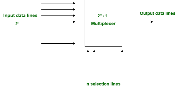
The multiplexer (MUX) functions as a multi-input and single-output switch. The selection of the input is done using select lines. A MUX with 2^n input lines have n select lines and is said to be a 2^n: 1 MUX with one output
Four-to-One Multiplexer:
This device has four inputs, two select pins, and one output with the truth table presented, select pins are represented by binary variables s0 and s1. Inputs are labeled as x0,x1,x2,x3. The output of the multiplexer is represented by binary variable y.


Verilog code for the simplest multiplexer, i.e. a 2:1 MUX.
Verilog code for a 2:1 MUX

Y = D0.S’ + D1.S
module m21(Y, D0, D1, S);
output Y;
input D0, D1, S;
wire T1, T2, Sbar;
and (T1, D1, S), (T2, D0, Sbar);
not (Sbar, S);
or (Y, T1, T2);
endmodule
using conditional operator:
module m21(D0, D1, S, Y);
output Y;
input D0, D1, S;
assign Y=(S)?D1:D0;
endmodule
using behavioural : if condition
module m21( D0, D1, S, Y);
input wire D0, D1, S;
output reg Y;

always @(D0 or D1 or S)
begin

if(S)
Y= D1;
else
Y=D0;

end

endmodule
Verilog code for 2:1 MUX using structural modelling

final code for 2:1 mux in structural style.
module and_gate(output a, input b, c);
assign a = b & c;
endmodule

module not_gate(output d, input e);
assign d = ~ e;
endmodule

module or_gate(output l, input m, n);
assign l = m | n;
endmodule

module m21(Y, D0, D1, S);
output Y;
input D0, D1, S;
wire T1, T2, T3;
and_gate u1(T1, D1, S);
not_gate u2(T2, S);
and_gate u3(T3, D0, T2);
or_gate u4(Y, T1, T3);
endmodule
similarly, we can do for 4:1,8:1 mux..........


No comments:
Post a Comment