MY CITATIONS

  • https://scholar.google.com/citations?user=8ke1xVQAAAAJ&hl=en
  • PREVIOUS QUESTION PAPERS : https://sircrrengg.ac.in/index.php?option=com_content&view=article&id=131&Itemid=459
  • YOUTUBE LINKS

Tuesday, December 21, 2021

Digital Safe System(using sequential circuit)

                         Digital Safe System(using sequential circuit)

In improved the digital safe system.

The user will have chance to enter his or her password instead of a fixed initial

value.

This module has five inputs.

·       clk (main clock signal),  

·       passinput (16-bit password)

·       pass_set (input to change password),

·       pass_reg (input to save new password)

·       pass_lock (to lock safe again after the password change).

The output of the module is a two-bit vector safestate. This output indicates the state of lock, such that

00 shows locked;

01 indicates open;

10 represents enter new password;

11 shows new password set.


Working principles of digital safe module (as a state machine) are as follows. The state machine has two states: ENTERPASS and SETPASS.

In ENTERPASS state, the machine checks whether the input matches the password.

If this is the case, safestate changes to 01 which shows that lock is open. Besides, if pass_set is at logic level 1, then state of the machine goes to SETPASS where the new password is entered. After the user determines a new password, pass_reg should go to logic level 1 to save it. Then, pass_lock should go to logic level 1 to lock the safe again.

We provide the modified Verilog description for the digital safe module

in CODE-1.


********************************************************************************

CODE-1

module digital_safe2(clk,passinput,pass_set,pass_reg,pass_lock,safestate);

input   clk;

input   [15:0]   passinput;

input   pass_set,pass_reg,pass_lock;

output   reg [1:0]   safestate;

//00:locked(c), 01:open(o), 10:enterpass, 11:pass changed(s)


localparam   ENTERPASS=1'b0,SETPASS=1'b1;

reg   [1:0]  state=ENTERPASS;

reg   [15:0]  pass=16'h1234;

always @ (posedge clk)

case(state)

ENTERPASS:     

            if (passinput == pass && pass_set == 1'b1)

            begin

            state <= SETPASS;

            safestate <= 2'b10;

            end

            else if (passinput == pass)

            safestate <= 2'b01;

            else safestate <= 2'b00;

SETPASS:

            if (pass_reg == 1'b1)

            begin

            pass <= passinput;

            safestate <= 2'b11; end

            else if (pass_lock == 1'b1)

            state <= ENTERPASS;

endcase

endmodule


********************************************************************************

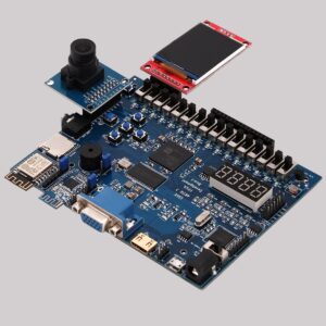
We can further improve the digital safe system to be implemented on the

FPGA board.

Here, we can show state of the lock and the new password on the seven-segment display. To do so, we should add the seven-segment display module as an IP block.

Inputs of the digital safe module will be connected to buttons and switches on the FPGA board. Hence, we should also add the debounce module as an IP block.

In CODE-2  pass_set, pass_reg, and pass_lock inputs are assigned to btnU, btnD, and btnC of the Basys3 board respectively. Sixteen switches are used as passinput. The master clock of the board is connected to clk signal.

The output safestate of the digital safe module is kept in a vector with the same name to control the seven-segment display on the board. Hence, when safestate is at 00 all four seven-segment display digits will show character C which stands for “Close”. When safestate is at 01, all display digits will show the character O which stands for “Open”. When safestate is at 11, all digits will show the character S which stands for “Set”. In the 01 state (referring to the password change), digits show the password while the user changes it.


We provide the top module for this application in CODE-2

.

********************************************************************************

CODE-2

module digital_safe_topmodule(clk,sw,btnC,btnU,btnD,led,an,seg);


input   clk;

input   [15:0]   sw;

input   btnC,btnU,btnD;

output   [1:0]   led;

output   [3:0]   an;

output   [6:0]   seg;


wire btnCclr,btnDclr,btnUclr;


debounce_0  dbc(clk,btnC,btnCclr);

debounce_0  dbu(clk,btnU,btnUclr);

debounce_0  dbd(clk,btnD,btnDclr);


reg   [3:0]  disp1=4'b0;

reg   [3:0]  disp2=4'b0;

reg   [3:0] disp3=4'b0;

reg   [3:0] disp4=4'b0;


sevenseg_driver_0  seg7(clk,1'b0,disp1,disp2,disp3,disp4,seg,an);


wire   [1:0]  safestate;


digital_safe2_0   ds(.clk(clk),.passinput(sw),.pass_set(btnUclr),.pass_reg(btnDclr),.pass_lock(btnCclr),.safestate(safestate));


always @ (posedge clk)

case(safestate)

2'b00 : {disp1,disp2,disp3,disp4} <= {4{4'b1100}}; //C

2'b01 : {disp1,disp2,disp3,disp4} <= {4{4'b0000}}; //0

2'b10 : {disp1,disp2,disp3,disp4} <= sw;

2'b11 : {disp1,disp2,disp3,disp4} <= {4{4'b0101}}; //S

endcase


assign led = safestate;


endmodule


********************************************************************************


Digital Safe System(FINAL MODULE)

We can finalize the digital safe system by adding a USB keyboard to it.Besides, the digital safe will work as explained in CODE 1 &2. We provide the modified and final form of the digital safe in CODE-3.

Let’s explain the working principles of the digital safe system (as a state machine) step by step. The system starts with a default password 1234. When the user enters it, the safe opens. Here, user has two options. The first one is changing the password. The second one is locking the safe again. When btnC on the Basys3 board is pressed, the safe locks again. If the user presses btnU, digital safe goes to the password changing state. Here, it expects the user to enter a new password. This can be done by using numbers on the keyboard. Since this is a prototype system, the entered password is also shown on the seven-segment display (and LEDs) of Basys3.When a new password is entered, the user should press btnD to save it. Afterward, btnC should be pressed to lock the safe again. While entering the password digits, the user may press btnR anytime to restart again.


********************************************************************************

CODE-3


module digital_safe_topmodule(clk,btnU,btnC,btnD,btnR,PS2Data,PS2Clk,seg,an,led);


input clk;

input btnC,btnU,btnD,btnR;

input PS2Data;

input PS2Clk;

output [3:0] an;

output [6:0] seg;

output [15:0] led;


wire btnCclr,btnDclr,btnUclr,btnRclr;


debounce_0 dbc(clk,btnC,btnCclr);

debounce_0 dbu(clk,btnU,btnUclr);

debounce_0 dbd(clk,btnD,btnDclr);

debounce_0 dbr(clk,btnR,btnRclr);


reg [3:0] disp1;

reg [3:0] disp2;

reg [3:0] disp3;

reg [3:0] disp4;


sevenseg_driver_0 seg7(clk,1'b0,disp1,disp2,disp3,disp4,seg,an);


wire [1:0] safestate;

reg [15:0] password;


digital_safe2_0 safe1(.clk(clk),.passinput(password),.pass_set(btnUclr),.pass_reg(btnDclr),.pass_lock(btnCclr),.safestate(safestate));


wire keyready;

reg keyready_prev;

reg [1:0] keystate=0;

wire [7:0] keyout;


keypad_app_0 key1(.clk(clk),.PS2Clk(PS2Clk),.PS2Data(PS2Data),.keyout(keyout),.ready(keyready));


always @ (posedge clk)

begin

keyready_prev <= keyready;

if (btnRclr) keystate <= 2'b0;

else if (btnCclr == 1'b1) password <= 16'b0;

else


case (keystate)

2'b00:     

          if (keyready_prev == 0 && keyready == 1) begin

          password[15:12] <= keyout;

          keystate <= keystate + 1'b1;

          end

2'b01:

          if (keyready_prev == 0 && keyready == 1) begin

          password[11:8] <= keyout;

          keystate <= keystate + 1'b1;

          end             

2'b10:     

          if (keyready_prev == 0 && keyready == 1) begin

          password[7:4] <= keyout;

          keystate <= keystate + 1'b1;

          end

2'b11:

          if (keyready_prev == 0 && keyready == 1) begin

          password[3:0] <= keyout;

          keystate <= 2'b00;

          end

endcase

end


always @ (posedge clk)

case(safestate)

          2'b00: {disp1,disp2,disp3,disp4} <= {4{4'b1100}}; //C

          2'b01: {disp1,disp2,disp3,disp4} <= {4{4'b0000}}; //0

          2'b10: {disp1,disp2,disp3,disp4} <= password;

          2'b11: {disp1,disp2,disp3,disp4} <= {4{4'b0101}}; //S

endcase


assign led = password;


endmodule


********************************************************************************


Monday, December 20, 2021

EDGE Artix 7 FPGA Development Board


EDGE Artix 7 FPGA Kit XDC Pin Details


## This file is a general .xdc for the EDGE Artix 7 board
## To use it in a project:
## - comment the lines corresponding to unused pins
## - rename the used ports (in each line, after get_ports) according to the top level signal names in the project
 
# Clock signal
set_property -dict { PACKAGE_PIN N11    IOSTANDARD LVCMOS33 } [get_ports { clk }];
 
# Switches
set_property -dict { PACKAGE_PIN L5    IOSTANDARD LVCMOS33 } [get_ports { sw[0] }];#LSB
set_property -dict { PACKAGE_PIN L4    IOSTANDARD LVCMOS33 } [get_ports { sw[1] }];
set_property -dict { PACKAGE_PIN M4    IOSTANDARD LVCMOS33 } [get_ports { sw[2] }];
set_property -dict { PACKAGE_PIN M2    IOSTANDARD LVCMOS33 } [get_ports { sw[3] }];
set_property -dict { PACKAGE_PIN M1    IOSTANDARD LVCMOS33 } [get_ports { sw[4] }];
set_property -dict { PACKAGE_PIN N3    IOSTANDARD LVCMOS33 } [get_ports { sw[5] }];
set_property -dict { PACKAGE_PIN N2    IOSTANDARD LVCMOS33 } [get_ports { sw[6] }];
set_property -dict { PACKAGE_PIN N1    IOSTANDARD LVCMOS33 } [get_ports { sw[7] }];
set_property -dict { PACKAGE_PIN P1    IOSTANDARD LVCMOS33 } [get_ports { sw[8] }];
set_property -dict { PACKAGE_PIN P4    IOSTANDARD LVCMOS33 } [get_ports { sw[9] }];
set_property -dict { PACKAGE_PIN T8    IOSTANDARD LVCMOS33 } [get_ports { sw[10] }];
set_property -dict { PACKAGE_PIN R8    IOSTANDARD LVCMOS33 } [get_ports { sw[11] }];
set_property -dict { PACKAGE_PIN N6    IOSTANDARD LVCMOS33 } [get_ports { sw[12] }];
set_property -dict { PACKAGE_PIN T7    IOSTANDARD LVCMOS33 } [get_ports { sw[13] }];
set_property -dict { PACKAGE_PIN P8    IOSTANDARD LVCMOS33 } [get_ports { sw[14] }];
set_property -dict { PACKAGE_PIN M6    IOSTANDARD LVCMOS33 } [get_ports { sw[15] }];#MSB
 
# LEDs
set_property -dict { PACKAGE_PIN J3    IOSTANDARD LVCMOS33 } [get_ports { led[0] }];#LSB
set_property -dict { PACKAGE_PIN H3    IOSTANDARD LVCMOS33 } [get_ports { led[1] }];
set_property -dict { PACKAGE_PIN J1    IOSTANDARD LVCMOS33 } [get_ports { led[2] }];
set_property -dict { PACKAGE_PIN K1    IOSTANDARD LVCMOS33 } [get_ports { led[3] }];
set_property -dict { PACKAGE_PIN L3    IOSTANDARD LVCMOS33 } [get_ports { led[4] }];
set_property -dict { PACKAGE_PIN L2    IOSTANDARD LVCMOS33 } [get_ports { led[5] }];
set_property -dict { PACKAGE_PIN K3    IOSTANDARD LVCMOS33 } [get_ports { led[6] }];
set_property -dict { PACKAGE_PIN K2    IOSTANDARD LVCMOS33 } [get_ports { led[7] }];
set_property -dict { PACKAGE_PIN K5    IOSTANDARD LVCMOS33 } [get_ports { led[8] }];
set_property -dict { PACKAGE_PIN P6    IOSTANDARD LVCMOS33 } [get_ports { led[9] }];
set_property -dict { PACKAGE_PIN R7    IOSTANDARD LVCMOS33 } [get_ports { led[10] }];
set_property -dict { PACKAGE_PIN R6    IOSTANDARD LVCMOS33 } [get_ports { led[11] }];
set_property -dict { PACKAGE_PIN T5    IOSTANDARD LVCMOS33 } [get_ports { led[12] }];
set_property -dict { PACKAGE_PIN R5    IOSTANDARD LVCMOS33 } [get_ports { led[13] }];
set_property -dict { PACKAGE_PIN T10   IOSTANDARD LVCMOS33 } [get_ports { led[14] }];
set_property -dict { PACKAGE_PIN T9    IOSTANDARD LVCMOS33 } [get_ports { led[15] }];#MSB
 
# Push Button
set_property -dict {PACKAGE_PIN K13 IOSTANDARD LVCMOS33 PULLDOWN true} [get_ports {pb[0]}]; #Button-top
set_property -dict {PACKAGE_PIN L14 IOSTANDARD LVCMOS33 PULLDOWN true} [get_ports {pb[1]}]; #Button-bottom
set_property -dict {PACKAGE_PIN M12 IOSTANDARD LVCMOS33 PULLDOWN true} [get_ports {pb[2]}]; #Button-left
set_property -dict {PACKAGE_PIN L13 IOSTANDARD LVCMOS33 PULLDOWN true} [get_ports {pb[3]}]; #Button-right
set_property -dict {PACKAGE_PIN M14 IOSTANDARD LVCMOS33 PULLDOWN true} [get_ports {pb[4]}]; #Button-center
 
#7 segment display
set_property -dict { PACKAGE_PIN F2    IOSTANDARD LVCMOS33 } [get_ports {digit[0]}]; #LSB
set_property -dict { PACKAGE_PIN E1    IOSTANDARD LVCMOS33 } [get_ports {digit[1]}];
set_property -dict { PACKAGE_PIN G5    IOSTANDARD LVCMOS33 } [get_ports {digit[2]}];
set_property -dict { PACKAGE_PIN G4    IOSTANDARD LVCMOS33 } [get_ports {digit[3]}]; #MSB
 
set_property -dict { PACKAGE_PIN G2    IOSTANDARD LVCMOS33 } [get_ports {Seven_Seg[0]}];#A
set_property -dict { PACKAGE_PIN G1    IOSTANDARD LVCMOS33 } [get_ports {Seven_Seg[1]}];#B
set_property -dict { PACKAGE_PIN H5    IOSTANDARD LVCMOS33 } [get_ports {Seven_Seg[2]}];#C
set_property -dict { PACKAGE_PIN H4    IOSTANDARD LVCMOS33 } [get_ports {Seven_Seg[3]}];#D
set_property -dict { PACKAGE_PIN J5    IOSTANDARD LVCMOS33 } [get_ports {Seven_Seg[4]}];#E
set_property -dict { PACKAGE_PIN J4    IOSTANDARD LVCMOS33 } [get_ports {Seven_Seg[5]}];#F
set_property -dict { PACKAGE_PIN H2    IOSTANDARD LVCMOS33 } [get_ports {Seven_Seg[6]}];#G
set_property -dict { PACKAGE_PIN H1    IOSTANDARD LVCMOS33 } [get_ports {Seven_Seg[7]}];#DP
 
# Bluetooth
set_property -dict { PACKAGE_PIN H14 IOSTANDARD LVCMOS33 } [get_ports { Bluetooth_txd }];
set_property -dict { PACKAGE_PIN J16 IOSTANDARD LVCMOS33 } [get_ports { Bluetooth_rxd }];
 
# Buzzer
set_property -dict { PACKAGE_PIN K12 IOSTANDARD LVCMOS33 } [get_ports {Buzzer}];
 
# SPI DAC (MCP4921)
set_property -dict { PACKAGE_PIN E5 IOSTANDARD LVCMOS33 } [get_ports {SCK}];
set_property -dict { PACKAGE_PIN F5 IOSTANDARD LVCMOS33 } [get_ports {CS}];
set_property -dict { PACKAGE_PIN F4 IOSTANDARD LVCMOS33 } [get_ports {MOSI}];
 
# HDMI
set_property -dict { PACKAGE_PIN A5 IOSTANDARD TMDS_33 } [get_ports {hdmi_tx_p[0]}];
set_property -dict { PACKAGE_PIN B6 IOSTANDARD TMDS_33 } [get_ports {hdmi_tx_p[1]}];
set_property -dict { PACKAGE_PIN B7 IOSTANDARD TMDS_33 } [get_ports {hdmi_tx_p[2]}];
set_property -dict { PACKAGE_PIN E3 IOSTANDARD TMDS_33 } [get_ports {hdmi_tx_clk_p}];
set_property -dict { PACKAGE_PIN A4 IOSTANDARD TMDS_33 } [get_ports {hdmi_tx_n[0]}];
set_property -dict { PACKAGE_PIN B5 IOSTANDARD TMDS_33 } [get_ports {hdmi_tx_n[1]}];
set_property -dict { PACKAGE_PIN A7 IOSTANDARD TMDS_33 } [get_ports {hdmi_tx_n[2]}];
set_property -dict { PACKAGE_PIN D3 IOSTANDARD TMDS_33 } [get_ports {hdmi_tx_clk_n}];
 
# 2x16 LCD
set_property -dict { PACKAGE_PIN P3 IOSTANDARD LVCMOS33 } [get_ports {data[7]}];
set_property -dict { PACKAGE_PIN M5 IOSTANDARD LVCMOS33 } [get_ports {data[6]}];
set_property -dict { PACKAGE_PIN N4 IOSTANDARD LVCMOS33 } [get_ports {data[5]}];
set_property -dict { PACKAGE_PIN R2 IOSTANDARD LVCMOS33 } [get_ports {data[4]}];
set_property -dict { PACKAGE_PIN R1 IOSTANDARD LVCMOS33 } [get_ports {data[3]}];
set_property -dict { PACKAGE_PIN R3 IOSTANDARD LVCMOS33 } [get_ports {data[2]}];
set_property -dict { PACKAGE_PIN T2 IOSTANDARD LVCMOS33 } [get_ports {data[1]}];
set_property -dict { PACKAGE_PIN T4 IOSTANDARD LVCMOS33 } [get_ports {data[0]}];
set_property -dict { PACKAGE_PIN T3 IOSTANDARD LVCMOS33 } [get_ports {lcd_e}];
set_property -dict { PACKAGE_PIN P5 IOSTANDARD LVCMOS33 } [get_ports {lcd_rs}];
#LCD R/W pin is connected to ground by default.No need to assign LCD R/W Pin.
 
#256Mb SDRAM (Only available with latest version of board)
set_property -dict { PACKAGE_PIN D8  IOSTANDARD LVCMOS33 } [get_ports { sdram_dq[0] }];
set_property -dict { PACKAGE_PIN C8  IOSTANDARD LVCMOS33 } [get_ports { sdram_dq[1] }];
set_property -dict { PACKAGE_PIN A8  IOSTANDARD LVCMOS33 } [get_ports { sdram_dq[2] }];
set_property -dict { PACKAGE_PIN A9  IOSTANDARD LVCMOS33 } [get_ports { sdram_dq[3] }];
set_property -dict { PACKAGE_PIN B9  IOSTANDARD LVCMOS33 } [get_ports { sdram_dq[4] }];
set_property -dict { PACKAGE_PIN A10 IOSTANDARD LVCMOS33 } [get_ports { sdram_dq[5] }];
set_property -dict { PACKAGE_PIN B10 IOSTANDARD LVCMOS33 } [get_ports { sdram_dq[6] }];
set_property -dict { PACKAGE_PIN C14 IOSTANDARD LVCMOS33 } [get_ports { sdram_dq[7] }];
set_property -dict { PACKAGE_PIN A14 IOSTANDARD LVCMOS33 } [get_ports { sdram_dq[8] }];
set_property -dict { PACKAGE_PIN A13 IOSTANDARD LVCMOS33 } [get_ports { sdram_dq[9] }];
set_property -dict { PACKAGE_PIN D9  IOSTANDARD LVCMOS33 } [get_ports { sdram_dq[10] }];
set_property -dict { PACKAGE_PIN D10 IOSTANDARD LVCMOS33 } [get_ports { sdram_dq[11] }];
set_property -dict { PACKAGE_PIN C9  IOSTANDARD LVCMOS33 } [get_ports { sdram_dq[12] }];
set_property -dict { PACKAGE_PIN A12 IOSTANDARD LVCMOS33 } [get_ports { sdram_dq[13] }];
set_property -dict { PACKAGE_PIN B12 IOSTANDARD LVCMOS33 } [get_ports { sdram_dq[14] }];
set_property -dict { PACKAGE_PIN B11 IOSTANDARD LVCMOS33 } [get_ports { sdram_dq[15] }];#MSB
 
set_property -dict { PACKAGE_PIN D11 IOSTANDARD LVCMOS33 } [get_ports { sdram_addr[0] }];#LSB
set_property -dict { PACKAGE_PIN E11 IOSTANDARD LVCMOS33 } [get_ports { sdram_addr[1] }];
set_property -dict { PACKAGE_PIN E13 IOSTANDARD LVCMOS33 } [get_ports { sdram_addr[2] }];
set_property -dict { PACKAGE_PIN D14 IOSTANDARD LVCMOS33 } [get_ports { sdram_addr[3] }];
set_property -dict { PACKAGE_PIN F3  IOSTANDARD LVCMOS33 } [get_ports { sdram_addr[4] }];
set_property -dict { PACKAGE_PIN G2  IOSTANDARD LVCMOS33 } [get_ports { sdram_addr[5] }];
set_property -dict { PACKAGE_PIN G1  IOSTANDARD LVCMOS33 } [get_ports { sdram_addr[6] }];
set_property -dict { PACKAGE_PIN H1  IOSTANDARD LVCMOS33 } [get_ports { sdram_addr[7] }];
set_property -dict { PACKAGE_PIN J5  IOSTANDARD LVCMOS33 } [get_ports { sdram_addr[8] }];
set_property -dict { PACKAGE_PIN H2  IOSTANDARD LVCMOS33 } [get_ports { sdram_addr[9] }];
set_property -dict { PACKAGE_PIN J4  IOSTANDARD LVCMOS33 } [get_ports { sdram_addr[10] }];
set_property -dict { PACKAGE_PIN H4  IOSTANDARD LVCMOS33 } [get_ports { sdram_addr[11] }];
set_property -dict { PACKAGE_PIN H5  IOSTANDARD LVCMOS33 } [get_ports { sdram_addr[12] }];
 
 
set_property -dict { PACKAGE_PIN B14 IOSTANDARD LVCMOS33 } [get_ports { sdram_ba[0] }];
set_property -dict { PACKAGE_PIN B15 IOSTANDARD LVCMOS33 } [get_ports { sdram_ba[1] }];
 
set_property -dict { PACKAGE_PIN E12 IOSTANDARD LVCMOS33 } [get_ports { sdram_dqm[0] }];
set_property -dict { PACKAGE_PIN C16 IOSTANDARD LVCMOS33 } [get_ports { sdram_dqm[1] }];
 
set_property -dict { PACKAGE_PIN D13 IOSTANDARD LVCMOS33 } [get_ports { sdram_clk }];
set_property -dict { PACKAGE_PIN A15 IOSTANDARD LVCMOS33 } [get_ports { sdram_cke }];
set_property -dict { PACKAGE_PIN C12 IOSTANDARD LVCMOS33 } [get_ports { sdram_cs_n }];
set_property -dict { PACKAGE_PIN C11 IOSTANDARD LVCMOS33 } [get_ports { sdram_we_n }];
set_property -dict { PACKAGE_PIN C13 IOSTANDARD LVCMOS33 } [get_ports { sdram_cas_n }];
set_property -dict { PACKAGE_PIN B16 IOSTANDARD LVCMOS33 } [get_ports { sdram_ras_n }];
 
# SPI TFT 1.8 inch
set_property -dict { PACKAGE_PIN T13 IOSTANDARD LVCMOS33 } [get_ports {tft_sck}];
set_property -dict { PACKAGE_PIN R10 IOSTANDARD LVCMOS33 } [get_ports {tft_sdi}];
set_property -dict { PACKAGE_PIN R11 IOSTANDARD LVCMOS33 } [get_ports {tft_dc}];
set_property -dict { PACKAGE_PIN N9  IOSTANDARD LVCMOS33 } [get_ports {tft_reset}];
set_property -dict { PACKAGE_PIN P9  IOSTANDARD LVCMOS33 } [get_ports {tft_cs}];
 
# USB UART
set_property -dict { PACKAGE_PIN C4 IOSTANDARD LVCMOS33 } [get_ports {usb_uart_txd}];
set_property -dict { PACKAGE_PIN D4 IOSTANDARD LVCMOS33 } [get_ports {usb_uart_rxd}];
 
# WiFi
set_property -dict { PACKAGE_PIN J15 IOSTANDARD LVCMOS33 } [get_ports { wifi_txd }];
set_property -dict { PACKAGE_PIN G16 IOSTANDARD LVCMOS33 } [get_ports { wifi_rxd }];
 
# CMOS Camera
set_property -dict { PACKAGE_PIN M16 IOSTANDARD LVCMOS33} [get_ports {ov7670_sioc}];
set_property -dict { PACKAGE_PIN N16 IOSTANDARD LVCMOS33} [get_ports {ov7670_siod}];
set_property -dict { PACKAGE_PIN P15 IOSTANDARD LVCMOS33} [get_ports {ov7670_vsync}];
set_property -dict { PACKAGE_PIN P16 IOSTANDARD LVCMOS33} [get_ports {ov7670_href}];
set_property -dict { PACKAGE_PIN R15 IOSTANDARD LVCMOS33} [get_ports {ov7670_pclk}];
set_property -dict { PACKAGE_PIN R16 IOSTANDARD LVCMOS33} [get_ports {ov7670_xclk}];
set_property -dict { PACKAGE_PIN T14 IOSTANDARD LVCMOS33} [get_ports {ov7670_data[7]}];
set_property -dict { PACKAGE_PIN T15 IOSTANDARD LVCMOS33} [get_ports {ov7670_data[6]}];
set_property -dict { PACKAGE_PIN N13 IOSTANDARD LVCMOS33} [get_ports {ov7670_data[5]}];
set_property -dict { PACKAGE_PIN P13 IOSTANDARD LVCMOS33} [get_ports {ov7670_data[4]}];
set_property -dict { PACKAGE_PIN N14 IOSTANDARD LVCMOS33} [get_ports {ov7670_data[3]}];
set_property -dict { PACKAGE_PIN P14 IOSTANDARD LVCMOS33} [get_ports {ov7670_data[2]}];
set_property -dict { PACKAGE_PIN P10 IOSTANDARD LVCMOS33} [get_ports {ov7670_data[1]}]; 
set_property -dict { PACKAGE_PIN P11 IOSTANDARD LVCMOS33} [get_ports {ov7670_data[0]}];
set_property -dict { PACKAGE_PIN R12 IOSTANDARD LVCMOS33} [get_ports {ov7670_reset}];
set_property -dict { PACKAGE_PIN T12 IOSTANDARD LVCMOS33} [get_ports {ov7670_pwdn}];
 
#20 pin expansion connector
#pin1 5V
#pin2 NC
#pin3 3V3
#pin4 GND
set_property -dict { PACKAGE_PIN M16 IOSTANDARD LVCMOS33} [get_ports {pin5}];
set_property -dict { PACKAGE_PIN N16 IOSTANDARD LVCMOS33} [get_ports {pin6}];
set_property -dict { PACKAGE_PIN P15 IOSTANDARD LVCMOS33} [get_ports {pin7}];
set_property -dict { PACKAGE_PIN P16 IOSTANDARD LVCMOS33} [get_ports {pin8}];
set_property -dict { PACKAGE_PIN R15 IOSTANDARD LVCMOS33} [get_ports {pin9}];
set_property -dict { PACKAGE_PIN R16 IOSTANDARD LVCMOS33} [get_ports {pin10}];
set_property -dict { PACKAGE_PIN T14 IOSTANDARD LVCMOS33} [get_ports {pin11}];
set_property -dict { PACKAGE_PIN T15 IOSTANDARD LVCMOS33} [get_ports {pin12}];
set_property -dict { PACKAGE_PIN N13 IOSTANDARD LVCMOS33} [get_ports {pin13}];     
set_property -dict { PACKAGE_PIN P13 IOSTANDARD LVCMOS33} [get_ports {pin14}];
set_property -dict { PACKAGE_PIN N14 IOSTANDARD LVCMOS33} [get_ports {pin15}];
set_property -dict { PACKAGE_PIN P14 IOSTANDARD LVCMOS33} [get_ports {pin16}];     
set_property -dict { PACKAGE_PIN P10 IOSTANDARD LVCMOS33} [get_ports {pin17];
set_property -dict { PACKAGE_PIN P11 IOSTANDARD LVCMOS33} [get_ports {pin18}];
set_property -dict { PACKAGE_PIN R12 IOSTANDARD LVCMOS33 } [get_ports {pin19}];   
set_property -dict { PACKAGE_PIN T12 IOSTANDARD LVCMOS33 } [get_ports {pin20}];
 
# VGA 12 bit
set_property -dict { PACKAGE_PIN F14 IOSTANDARD LVCMOS33 } [get_ports {vga_hsync}];
set_property -dict { PACKAGE_PIN H16 IOSTANDARD LVCMOS33 } [get_ports {vga_vsync}];
set_property -dict { PACKAGE_PIN D15 IOSTANDARD LVCMOS33 } [get_ports {vga_r[0]}];
set_property -dict { PACKAGE_PIN F12 IOSTANDARD LVCMOS33 } [get_ports {vga_r[1]}];
set_property -dict { PACKAGE_PIN F13 IOSTANDARD LVCMOS33 } [get_ports {vga_r[2]}];
set_property -dict { PACKAGE_PIN E16 IOSTANDARD LVCMOS33 } [get_ports {vga_r[3]}];
set_property -dict { PACKAGE_PIN D16 IOSTANDARD LVCMOS33 } [get_ports {vga_g[0]}];
set_property -dict { PACKAGE_PIN F15 IOSTANDARD LVCMOS33 } [get_ports {vga_g[1]}];
set_property -dict { PACKAGE_PIN E15 IOSTANDARD LVCMOS33 } [get_ports {vga_g[2]}];
set_property -dict { PACKAGE_PIN H11 IOSTANDARD LVCMOS33 } [get_ports {vga_g[3]}];
set_property -dict { PACKAGE_PIN G12 IOSTANDARD LVCMOS33 } [get_ports {vga_b[0]}];
set_property -dict { PACKAGE_PIN H12 IOSTANDARD LVCMOS33 } [get_ports {vga_b[1]}];
set_property -dict { PACKAGE_PIN H13 IOSTANDARD LVCMOS33 } [get_ports {vga_b[2]}];
set_property -dict { PACKAGE_PIN G14 IOSTANDARD LVCMOS33 } [get_ports {vga_b[3]}];
 
# SD Card
set_property -dict { PACKAGE_PIN D6  IOSTANDARD LVCMOS33 } [get_ports {sd_cclk}];
set_property -dict { PACKAGE_PIN E6  IOSTANDARD LVCMOS33 } [get_ports {sd_cd}]}];
set_property -dict { PACKAGE_PIN D5  IOSTANDARD LVCMOS33 } [get_ports {sd_cmd}]}];
set_property -dict { PACKAGE_PIN B4  IOSTANDARD LVCMOS33 } [get_ports {sd_d[0]}];
set_property -dict { PACKAGE_PIN A3  IOSTANDARD LVCMOS33 } [get_ports {sd_d[1]}];
set_property -dict { PACKAGE_PIN C7  IOSTANDARD LVCMOS33 } [get_ports {sd_d[2]}];
set_property -dict { PACKAGE_PIN C6  IOSTANDARD LVCMOS33 } [get_ports {sd_d[3]}];
 
# XADC Single Ended Input available at J13 Connector
set_property -dict { PACKAGE_PIN C3  IOSTANDARD LVCMOS33 } [get_ports {vauxp6}];
set_property -dict { PACKAGE_PIN C2  IOSTANDARD LVCMOS33 } [get_ports {vauxn6}];
set_property -dict { PACKAGE_PIN B2  IOSTANDARD LVCMOS33 } [get_ports {vauxp14}];   
set_property -dict { PACKAGE_PIN A2  IOSTANDARD LVCMOS33 } [get_ports {vauxn14}];  
set_property -dict { PACKAGE_PIN C1  IOSTANDARD LVCMOS33 } [get_ports {vauxp7}] ;
set_property -dict { PACKAGE_PIN B1  IOSTANDARD LVCMOS33 } [get_ports {vauxn7}];
set_property -dict { PACKAGE_PIN E2  IOSTANDARD LVCMOS33 } [get_ports {vauxp15}];   
set_property -dict { PACKAGE_PIN D1  IOSTANDARD LVCMOS33 } [get_ports {vauxn15}];  
     
# Audio Jack
set_property -dict { PACKAGE_PIN G11  IOSTANDARD LVCMOS33 } [get_ports { Audio_L }];    
set_property -dict { PACKAGE_PIN G15  IOSTANDARD LVCMOS33 } [get_ports { Audio_R }];   
     
# SRAM 512 KB  (SRAM replaced with SDRAM in the latest version of board) only required for older boards
#set_property -dict { PACKAGE_PIN D10 IOSTANDARD LVCMOS33 } [get_ports {sram_addr[0]}];
#set_property -dict { PACKAGE_PIN C8 IOSTANDARD LVCMOS33  } [get_ports {sram_addr[1]}];
#set_property -dict { PACKAGE_PIN C9 IOSTANDARD LVCMOS33  } [get_ports {sram_addr[2]}];
#set_property -dict { PACKAGE_PIN A8 IOSTANDARD LVCMOS33  } [get_ports {sram_addr[3]}];
#set_property -dict { PACKAGE_PIN A9 IOSTANDARD LVCMOS33  } [get_ports {sram_addr[4]}];
#set_property -dict { PACKAGE_PIN B9 IOSTANDARD LVCMOS33  } [get_ports {sram_addr[5]}];
#set_property -dict { PACKAGE_PIN A10 IOSTANDARD LVCMOS33 } [get_ports {sram_addr[6]}];
#set_property -dict { PACKAGE_PIN B10 IOSTANDARD LVCMOS33 } [get_ports {sram_addr[7]}];
#set_property -dict { PACKAGE_PIN B11 IOSTANDARD LVCMOS33 } [get_ports {sram_addr[8]}];
#set_property -dict { PACKAGE_PIN B12 IOSTANDARD LVCMOS33 } [get_ports {sram_addr[9]}];
#set_property -dict { PACKAGE_PIN A12 IOSTANDARD LVCMOS33 } [get_ports {sram_addr[10]}];
#set_property -dict { PACKAGE_PIN D8 IOSTANDARD LVCMOS33  } [get_ports {sram_addr[11]}];
#set_property -dict { PACKAGE_PIN D9 IOSTANDARD LVCMOS33  } [get_ports {sram_addr[12]}];
#set_property -dict { PACKAGE_PIN A13 IOSTANDARD LVCMOS33 } [get_ports {sram_addr[13]}];
#set_property -dict { PACKAGE_PIN A14 IOSTANDARD LVCMOS33 } [get_ports {sram_addr[14]}];
#set_property -dict { PACKAGE_PIN C14 IOSTANDARD LVCMOS33 } [get_ports {sram_addr[15]}];
#set_property -dict { PACKAGE_PIN B14 IOSTANDARD LVCMOS33 } [get_ports {sram_addr[16]}];
#set_property -dict { PACKAGE_PIN B15 IOSTANDARD LVCMOS33 } [get_ports {sram_addr[17]}];
#set_property -dict { PACKAGE_PIN A15 IOSTANDARD LVCMOS33 } [get_ports {sram_addr[18]}];
 
#set_property -dict { PACKAGE_PIN C16 IOSTANDARD LVCMOS33 } [get_ports {sram_data[0]}];
#set_property -dict { PACKAGE_PIN B16 IOSTANDARD LVCMOS33 } [get_ports {sram_data[1]}];
#set_property -dict { PACKAGE_PIN C11 IOSTANDARD LVCMOS33 } [get_ports {sram_data[2]}];
#set_property -dict { PACKAGE_PIN C12 IOSTANDARD LVCMOS33 } [get_ports {sram_data[3]}];
#set_property -dict { PACKAGE_PIN D13 IOSTANDARD LVCMOS33 } [get_ports {sram_data[4]}];
#set_property -dict { PACKAGE_PIN C13 IOSTANDARD LVCMOS33 } [get_ports {sram_data[5]}];
#set_property -dict { PACKAGE_PIN E12 IOSTANDARD LVCMOS33 } [get_ports {sram_data[6]}];
#set_property -dict { PACKAGE_PIN E13 IOSTANDARD LVCMOS33 } [get_ports {sram_data[7]}];
 
#set_property -dict { PACKAGE_PIN D14 IOSTANDARD LVCMOS33 } [get_ports {sram_we_n}];
#set_property -dict { PACKAGE_PIN E11 IOSTANDARD LVCMOS33 } [get_ports {sram_oe_n}];
#set_property -dict { PACKAGE_PIN D11 IOSTANDARD LVCMOS33 } [get_ports {sram_ce_a_n}];


DICD MID-2 IMP QUESTION

   ̅ What is a bistable element? Design bistable device with the help of CMOS inverters and also discuss transient analysis . Design a...