Unit 3: Part 1
Combinational Circuits
Combinational Circuit Analysis:
Logic gates can be used to construct combinational circuits. To understand the working principles of a combinational circuit, we should analyze it. Therefore, we should first form a logic function between its inputs and output(s). If needed, we can also form the truth table of combinational circuit based on this representation. The final step in the analysis is representing the combinational circuit by less (or simpler) elements, which is called gate-level minimization.
- Logic Function Formation between Input and Output
- Boolean Algebra
- Gate-Level Minimization
- Combinational Circuit Implementation: Truth Table-Based Implementation
- Combinational Circuit Design


These lead to input/output characteristics of the combinational circuit as follows:
Boolean Algebra is used to analyze and simplify the digital (logic) circuits. It uses only the binary numbers i.e. 0 and 1. It is also called as Binary Algebra or logical Algebra. Boolean algebra was invented by George Boole in 1854.
Rule in Boolean Algebra
Following are the important rules used in Boolean algebra.
- The variable used can have only two values. Binary 1 for HIGH and Binary 0 for LOW.
- Complement of a variable is represented by an overbar (-). Thus, complement of variable B is represented as
 . Thus if B = 0 then = 1 and B = 1 then = 0.
 - ORing of the variables is represented by a plus (+) sign between them. For example ORing of A, B, C is represented as A + B + C.
- Logical ANDing of the two or more variable is represented by writing a dot between them such as A.B.C. Sometimes the dot may be omitted like ABC.
Boolean Laws
There are six types of Boolean Laws.
Commutative law
Any binary operation which satisfies the following expression is referred to as a commutative operation.
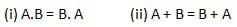
Commutative law states that changing the sequence of the variables does not have any effect on the output of a logic circuit.
Associative law
This law states that the order in which the logic operations are performed is irrelevant as their effect is the same.

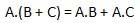
Distributive law
Distributive law states the following condition.
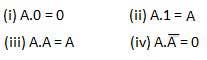
AND law
These laws use the AND operation. Therefore they are called as AND laws.
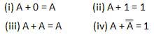
OR law
These laws use the OR operation. Therefore they are called as OR laws.
INVERSION law
This law uses the NOT operation. The inversion law states that double inversion of a variable results in the original variable itself.

De Morgan's Theorems:
De Morgan has suggested two theorems that are extremely useful in Boolean Algebra. The two theorems are discussed below.
Theorem 1
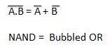 The left-hand side (LHS) of this theorem represents a NAND gate with inputs A and B, whereas the right-hand side (RHS) of the theorem represents an OR gate with inverted inputs.
This OR gate is called a Bubbled OR.
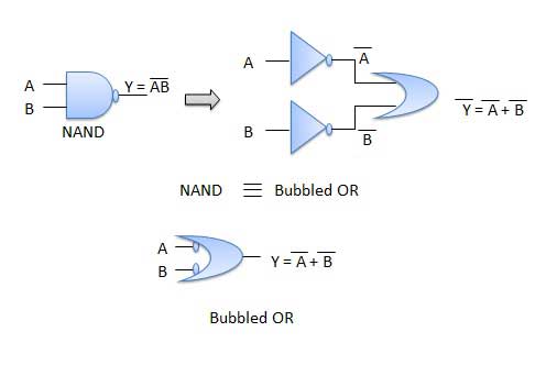
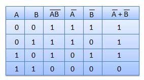
Table showing verification of the De Morgan's first theorem −
Theorem 2
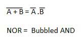 The LHS of this theorem represents a NOR gate with inputs A and B, whereas the RHS represents an AND gate with inverted inputs.
This AND gate is called a Bubbled AND.
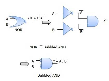
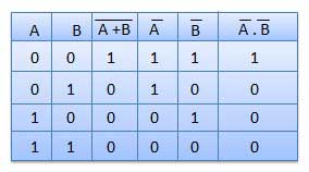
Table showing verification of the De Morgan's second theorem −

example: Boolean Identity Operations in Verilog


Gate-level minimization example in Vivado


No comments:
Post a Comment