Thursday, November 4, 2021

Implementing the Car Park Occupied Slot Counting System

 Car Park Occupied Slot Counting System

Problem definition:

There is a car park with three slots and we would like to know how many of its slots are occupied at a given time. Within the design, occupied slot locations are not important.

Solution:

We can design a combinational circuit for this purpose. 

Assume that we placed a sensor over each slot which gives output logic level 1 when the slot is occupied. If the slot is empty, sensor gives output logic level 0.

 Let’s label output of sensors as binary variables s0, s1, and s2. 

The designed combinational circuit will provide the output as a two-bit binary number c1 (MSB) and c0 (LSB). Therefore, we should cover all input combinations in terms of a truth table


                                Truth Table of the Car Park Occupied Slot Counting System

logic functions for c0 and c1 in the SOP form as follows:


Verilog Description of the Car Park Occupied Slot Counting System code:1


Synthesization result of the car park occupied slot counting system


Implementing the Digital Safe System

  Digital Safe System

Problem Definition:

We can design a simple digital safe using combinational circuits. Assume that the system has a four-bit predefined password. We will use four switches as the input to the system. If the input matches the predefined password, then the first output will have logic level 1. Otherwise, the second output will have logic level 1.

solution:

We can implement the corresponding combinational circuit using an XOR gate followed by a NOT gate for each bit to be tested. Therefore, if input bit matches the corresponding password bit, then the XOR gate followed by NOT will give logic level 1. If all input bits match corresponding predefined password bits this way, the first output will have logic level 1 and the second output will have logic level 0. The second output will simply be inverse of the first output.

To implement the combinational circuit for the design,

let’s assign binary variables s0, s1, s2, and s3 as input. 

Predefined password can be represented as p[0] · · · p[3].

 Let’s define the first and second outputs as binary variables l0 and l1, respectively. 

The logic function between the inputs and first output variable will be


The 
second output will be   l1 = ~ lo


Circuit diagram of the digital safe system
code:1

Verilog Description of the Digital Safe System  
code:1


Synthesization result of the digital safe system

we can be seen in this figure, two four-input LUTs are sufficient for implementation.

Implementing the Home Alarm System

  Home Alarm System

Problem definition:

Assume that the alarm system to be designed is to be applied on three windows and a door. Each window and the door has a sensor such that when it is opened, it will give logic level 1. There should be an on/off switch for the alarm. If we want to activate the alarm, the switch will give logic level 1. Otherwise, it will give logic level 0.

solution : 

Implementing the combinational circuit for the design problem.

  1. Let’s assign binary variables s0, s1, s2, and s3 to each sensor output.
  2. Let the on/off switch be represented by the binary variable m.
  3. Let’s define the binary variable a as an output. This variable will have logic value 1 when an intruder triggers the alarm. Otherwise, the output of the system will be logic level 0. 

Based on all these constraints, the logic function between the input and output will be

                                            a = (s0 + s1 + s2 + s3) · m.


Circuit diagram of the home alarm system.

Verilog Description of the Home Alarm System:( code:1)


Synthesization result of the home alarm system.


================================================


we can implement home alarm system designs on the Basys3 board.

we provide the Verilog description in which LEDs and switches on the board are connected as the input and output in code 2. Here, we use the Verilog description of the system in code:1 as an IP block.

Home Alarm System Implemented on the Basys3 Board in Verilog code 2


Improving the Home Alarm System

The home alarm system can be improved by using a seven-segment display. When the home alarm system is active, the display will show character A. When it is closed, the display will show character 0 . To do so, we should add a seven-segment display decoder module to the system. This module converts the provided hexadecimal number to the corresponding seven-segment display pattern

We provide the Verilog description of the seven-segment display decoder module. We should form an IP block for this module to be used in the application.

Verilog Description of the Seven-Segment Display Decoder Module code 3


Improved Home Alarm System Implemented on the Basys3 Board in Verilog code 4


We provide the modified Verilog description for the application in code 4. Here, the home alarm system in code 1 is taken as an IP block. Therefore, we assume that the reader has converted it to an IP block and added it to the project.


 Home Alarm System (Using sequential circuits)

         ðŸ‘‰ back to combination blocks

Parity Generators and Checkers in Verilog

 Parity Generators and Checkers in Verilog


    While transferring or storing binary data, some bit values may change because of a physical effect or an unpredicted disturbance. 

    To check whether such an undesired change has occurred or not, extra bits can be added to the data. This is called parity generation. 

Parity Generators:

In parity, generation is adding an extra bit to set the total number of bits in a binary data block as even or odd. 

The idea here is as follows. If a bit value changes from logic level 1 to 0 (or vice versa) by an undesired effect, the total number of even (or odd) bits will not satisfy the initial condition.

There are two options here.

 The first option is setting the total number of ones to be even. This is called even parity. 

The second option is setting the total number of ones to be odd. This is called odd parity.

example: consider three-bit data.

the three-bit data is represented by binary variables b0, b1, and b2. The generated even-parity bit is represented by binary variable pe.


Truth Table of Three-Bit Even-Parity Generator

The even-parity bit can be generated by the logic function 

                    pe = b0 ⊕ b1 ⊕ b2.

The even-parity generator can be composed of two XOR gates with two inputs


    Circuit diagram of three-bit even-parity generator

Verilog Description of Three-Bit Even-Parity Generator:


Parity Checkers:

After adding a parity bit, we can construct a combinational circuit to check whether an undesired change has occurred in the data during transmission or storage.

 To do so, we can use the same circuitry as in the parity generator with an additional parity bit. This is called parity checker

Parity checker circuitry can be constructed by logic function 
                            C =b0 ⊕ b1 ⊕ b2  ⊕ pe

Circuit diagram of three-bit even-parity checker


Verilog Description of Three-Bit Even-Parity Checker


                                   ðŸ‘‰ back to combination blocks

Multiplexer in verilog


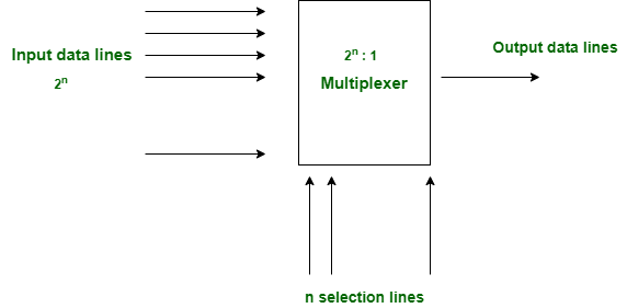
    A multiplexer is a device that selects one output from multiple inputs. It is also known as a data selector. Multiplexers are used in communication systems to increase the amount of data that can be sent over a network within a certain amount of time and bandwidth. It allows us to ‘squeeze’ multiple data lines into one data line.

The multiplexer (MUX) functions as a multi-input and single-output switch. The selection of the input is done using select lines. A MUX with 2^n input lines have n select lines and is said to be a 2^n: 1 MUX with one output


Four-to-One Multiplexer:

This device has four inputs, two select pins, and one output with the truth table presented, select pins are represented by binary variables s0 and s1. Inputs are labeled as x0,x1,x2,x3. The output of the multiplexer is represented by binary variable y.

Truth Table of Four-to-One Multiplexer 
Circuit diagram of a four-to-one multiplexer

Verilog Description of Four-to-One Multiplexer:

Verilog code for the simplest multiplexer, i.e. a 2:1 MUX.


Verilog code for a 2:1 MUX


                                            Y = D0.S’ + D1.S
module m21(Y, D0, D1, S);
output Y;
input D0, D1, S;
wire T1, T2, Sbar;
and (T1, D1, S), (T2, D0, Sbar);
not (Sbar, S);
or (Y, T1, T2);
endmodule

using conditional operator:

module m21(D0, D1, S, Y);
output Y;
input D0, D1, S;
assign Y=(S)?D1:D0;
endmodule

using behavioural : if condition

module m21( D0, D1, S, Y);
input wire D0, D1, S;
output reg Y;

always @(D0 or D1 or S)
begin

if(S) 
Y= D1;
else
Y=D0;

end

endmodule

Verilog code for 2:1 MUX using structural modelling


final code for 2:1 mux in structural style.

module and_gate(output a, input b, c);
assign a = b & c;
endmodule

module not_gate(output d, input e);
assign d = ~ e;
endmodule

module or_gate(output l, input m, n);
assign l = m | n;
endmodule

module m21(Y, D0, D1, S);
output Y;
input D0, D1, S;
wire T1, T2, T3;
and_gate u1(T1, D1, S);
not_gate u2(T2, S);
and_gate u3(T3, D0, T2);
or_gate u4(Y, T1, T3);
endmodule
similarly, we can do for 4:1,8:1 mux..........


👉 back to combination blocks

Monday, November 1, 2021

Encoders in Verilog

 Encoders in Verilog


The encoder works just as the opposite of the decoder. Its function is to encode a given input and provide encoded output. In general, an encoder has at most 2N inputs and N outputs. Let’s focus on the four-to-two encoder with the truth table presented.

Truth Table of the Four-to-Two Encoder

The output of the encoder is the binary representation of the input. While constructing the truth table, we assumed that no two inputs will have logic level 1 at the same time. If such a case occurs, then the output of the decoder becomes unpredictable. 

    To overcome this problem, we can add priority to inputs such that the output is the one with the higher precedence.


Octal to Binary Encoder

Octal to binary Encoder has eight inputs, Y7 to Y0 and three outputs A2, A1 & A0. Octal to binary encoder is nothing but 8 to 3 encoder. The block diagram of octal to binary Encoder is shown in the following figure.
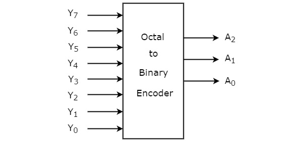
Octal to Binary Encoder

At any time, only one of these eight inputs can be ‘1’ in order to get the respective binary code. The Truth table of octal to binary encoder is shown below.

InputsOutputs
Y7Y6Y5Y4Y3Y2Y1Y0A2A1A0
00000001000
00000010001
00000100010
00001000011
00010000100
00100000101
01000000110
10000000111

From Truth table, we can write the Boolean functions for each output as


We can implement the above Boolean functions by using four input OR gates. The circuit diagram of octal to binary encoder is shown in the following figure.
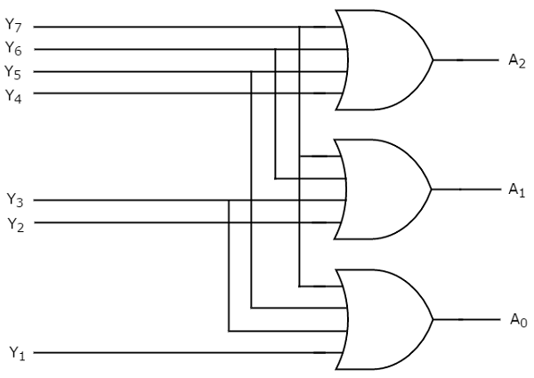
Octal to Binary Encoder Circuit Diagram

The above circuit diagram contains three 4-input OR gates. These OR gates encode the eight inputs with three bits.

Drawbacks of Encoder

Following are the drawbacks of normal encoder.

  • There is an ambiguity, when all outputs of encoder are equal to zero. Because, it could be the code corresponding to the inputs, when only least significant input is one or when all inputs are zero.

  • If more than one input is active High, then the encoder produces an output, which may not be the correct code. For example, if both Y3 and Y6 are ‘1’, then the encoder produces 111 at the output. This is neither equivalent code corresponding to Y3, when it is ‘1’ nor the equivalent code corresponding to Y6, when it is ‘1’.

So, to overcome these difficulties, we should assign priorities to each input of encoder. Then, the output of encoder will be the binary code corresponding to the active High inputs, which has higher priority. This encoder is called as priority encoder.

Priority Encoder

Four-to-Two Priority Encoder:

    Within the priority encoder, we still assume that all inputs will not be zero at the same time. To check whether such an input comes, we can add a valid signal, v, to the output. This will indicate that the obtained output is either valid or not. Here don’t care conditions are represented by “ - “ sign.


Truth Table of Four-to-Two Priority Encoder

we can construct the combinational circuit of the four-to-two priority encoder as follows:

A 4 to 2 priority encoder has four inputs X3, X2, X1 & X0 and two outputs A1 & A0. Here, the input, X3 has the highest priority, whereas the input, Y0 has the lowest priority. 

In this case, even if more than one input is ‘1’ at the same time, the output will be the binary code corresponding to the input, which is having higher priority.

We considered one more output, V in order to know, whether the code available at outputs is valid or not.

  • If at least one input of the encoder is ‘1’, then the code available at outputs is a valid one. In this case, the output, V will be equal to 1.

  • If all the inputs of encoder are ‘0’, then the code available at outputs is not a valid one. In this case, the output, V will be equal to 0.


Use 4 variable K-maps for getting simplified expressions for each output.


The simplified Boolean functions are


We can implement the above Boolean functions using logic gates. The circuit diagram of 4 to 2 priority encoder is shown in the following figure.


Verilog Description of Four-to-Two Priority Encoder


👉 back to combination blocks

STLD QUESTION BANK & SOLUTION

 STLD mid-1 solution https://docs.google.com/document/d/1RkU6RE-COZCG_MY4oCihimX4muc9jJM9/edit?usp=drivesdk&ouid=102051422039972401246...