EDGE Artix 7 FPGA Kit XDC Pin Details
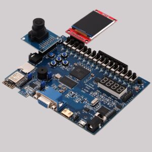
## This file is a general .xdc for the EDGE Artix 7 board |
## To use it in a project: |
## - comment the lines corresponding to unused pins |
## - rename the used ports (in each line, after get_ports) according to the top level signal names in the project |
# Clock signal |
set_property -dict { PACKAGE_PIN N11 IOSTANDARD LVCMOS33 } [get_ports { clk }]; |
# Switches |
set_property -dict { PACKAGE_PIN L5 IOSTANDARD LVCMOS33 } [get_ports { sw[0] }];#LSB |
set_property -dict { PACKAGE_PIN L4 IOSTANDARD LVCMOS33 } [get_ports { sw[1] }]; |
set_property -dict { PACKAGE_PIN M4 IOSTANDARD LVCMOS33 } [get_ports { sw[2] }]; |
set_property -dict { PACKAGE_PIN M2 IOSTANDARD LVCMOS33 } [get_ports { sw[3] }]; |
set_property -dict { PACKAGE_PIN M1 IOSTANDARD LVCMOS33 } [get_ports { sw[4] }]; |
set_property -dict { PACKAGE_PIN N3 IOSTANDARD LVCMOS33 } [get_ports { sw[5] }]; |
set_property -dict { PACKAGE_PIN N2 IOSTANDARD LVCMOS33 } [get_ports { sw[6] }]; |
set_property -dict { PACKAGE_PIN N1 IOSTANDARD LVCMOS33 } [get_ports { sw[7] }]; |
set_property -dict { PACKAGE_PIN P1 IOSTANDARD LVCMOS33 } [get_ports { sw[8] }]; |
set_property -dict { PACKAGE_PIN P4 IOSTANDARD LVCMOS33 } [get_ports { sw[9] }]; |
set_property -dict { PACKAGE_PIN T8 IOSTANDARD LVCMOS33 } [get_ports { sw[10] }]; |
set_property -dict { PACKAGE_PIN R8 IOSTANDARD LVCMOS33 } [get_ports { sw[11] }]; |
set_property -dict { PACKAGE_PIN N6 IOSTANDARD LVCMOS33 } [get_ports { sw[12] }]; |
set_property -dict { PACKAGE_PIN T7 IOSTANDARD LVCMOS33 } [get_ports { sw[13] }]; |
set_property -dict { PACKAGE_PIN P8 IOSTANDARD LVCMOS33 } [get_ports { sw[14] }]; |
set_property -dict { PACKAGE_PIN M6 IOSTANDARD LVCMOS33 } [get_ports { sw[15] }];#MSB |
# LEDs |
set_property -dict { PACKAGE_PIN J3 IOSTANDARD LVCMOS33 } [get_ports { led[0] }];#LSB |
set_property -dict { PACKAGE_PIN H3 IOSTANDARD LVCMOS33 } [get_ports { led[1] }]; |
set_property -dict { PACKAGE_PIN J1 IOSTANDARD LVCMOS33 } [get_ports { led[2] }]; |
set_property -dict { PACKAGE_PIN K1 IOSTANDARD LVCMOS33 } [get_ports { led[3] }]; |
set_property -dict { PACKAGE_PIN L3 IOSTANDARD LVCMOS33 } [get_ports { led[4] }]; |
set_property -dict { PACKAGE_PIN L2 IOSTANDARD LVCMOS33 } [get_ports { led[5] }]; |
set_property -dict { PACKAGE_PIN K3 IOSTANDARD LVCMOS33 } [get_ports { led[6] }]; |
set_property -dict { PACKAGE_PIN K2 IOSTANDARD LVCMOS33 } [get_ports { led[7] }]; |
set_property -dict { PACKAGE_PIN K5 IOSTANDARD LVCMOS33 } [get_ports { led[8] }]; |
set_property -dict { PACKAGE_PIN P6 IOSTANDARD LVCMOS33 } [get_ports { led[9] }]; |
set_property -dict { PACKAGE_PIN R7 IOSTANDARD LVCMOS33 } [get_ports { led[10] }]; |
set_property -dict { PACKAGE_PIN R6 IOSTANDARD LVCMOS33 } [get_ports { led[11] }]; |
set_property -dict { PACKAGE_PIN T5 IOSTANDARD LVCMOS33 } [get_ports { led[12] }]; |
set_property -dict { PACKAGE_PIN R5 IOSTANDARD LVCMOS33 } [get_ports { led[13] }]; |
set_property -dict { PACKAGE_PIN T10 IOSTANDARD LVCMOS33 } [get_ports { led[14] }]; |
set_property -dict { PACKAGE_PIN T9 IOSTANDARD LVCMOS33 } [get_ports { led[15] }];#MSB |
# Push Button |
set_property -dict {PACKAGE_PIN K13 IOSTANDARD LVCMOS33 PULLDOWN true} [get_ports {pb[0]}]; #Button-top |
set_property -dict {PACKAGE_PIN L14 IOSTANDARD LVCMOS33 PULLDOWN true} [get_ports {pb[1]}]; #Button-bottom |
set_property -dict {PACKAGE_PIN M12 IOSTANDARD LVCMOS33 PULLDOWN true} [get_ports {pb[2]}]; #Button-left |
set_property -dict {PACKAGE_PIN L13 IOSTANDARD LVCMOS33 PULLDOWN true} [get_ports {pb[3]}]; #Button-right |
set_property -dict {PACKAGE_PIN M14 IOSTANDARD LVCMOS33 PULLDOWN true} [get_ports {pb[4]}]; #Button-center |
#7 segment display |
set_property -dict { PACKAGE_PIN F2 IOSTANDARD LVCMOS33 } [get_ports {digit[0]}]; #LSB |
set_property -dict { PACKAGE_PIN E1 IOSTANDARD LVCMOS33 } [get_ports {digit[1]}]; |
set_property -dict { PACKAGE_PIN G5 IOSTANDARD LVCMOS33 } [get_ports {digit[2]}]; |
set_property -dict { PACKAGE_PIN G4 IOSTANDARD LVCMOS33 } [get_ports {digit[3]}]; #MSB |
set_property -dict { PACKAGE_PIN G2 IOSTANDARD LVCMOS33 } [get_ports {Seven_Seg[0]}];#A |
set_property -dict { PACKAGE_PIN G1 IOSTANDARD LVCMOS33 } [get_ports {Seven_Seg[1]}];#B |
set_property -dict { PACKAGE_PIN H5 IOSTANDARD LVCMOS33 } [get_ports {Seven_Seg[2]}];#C |
set_property -dict { PACKAGE_PIN H4 IOSTANDARD LVCMOS33 } [get_ports {Seven_Seg[3]}];#D |
set_property -dict { PACKAGE_PIN J5 IOSTANDARD LVCMOS33 } [get_ports {Seven_Seg[4]}];#E |
set_property -dict { PACKAGE_PIN J4 IOSTANDARD LVCMOS33 } [get_ports {Seven_Seg[5]}];#F |
set_property -dict { PACKAGE_PIN H2 IOSTANDARD LVCMOS33 } [get_ports {Seven_Seg[6]}];#G |
set_property -dict { PACKAGE_PIN H1 IOSTANDARD LVCMOS33 } [get_ports {Seven_Seg[7]}];#DP |
# Bluetooth |
set_property -dict { PACKAGE_PIN H14 IOSTANDARD LVCMOS33 } [get_ports { Bluetooth_txd }]; |
set_property -dict { PACKAGE_PIN J16 IOSTANDARD LVCMOS33 } [get_ports { Bluetooth_rxd }]; |
# Buzzer |
set_property -dict { PACKAGE_PIN K12 IOSTANDARD LVCMOS33 } [get_ports {Buzzer}]; |
# SPI DAC (MCP4921) |
set_property -dict { PACKAGE_PIN E5 IOSTANDARD LVCMOS33 } [get_ports {SCK}]; |
set_property -dict { PACKAGE_PIN F5 IOSTANDARD LVCMOS33 } [get_ports {CS}]; |
set_property -dict { PACKAGE_PIN F4 IOSTANDARD LVCMOS33 } [get_ports {MOSI}]; |
# HDMI |
set_property -dict { PACKAGE_PIN A5 IOSTANDARD TMDS_33 } [get_ports {hdmi_tx_p[0]}]; |
set_property -dict { PACKAGE_PIN B6 IOSTANDARD TMDS_33 } [get_ports {hdmi_tx_p[1]}]; |
set_property -dict { PACKAGE_PIN B7 IOSTANDARD TMDS_33 } [get_ports {hdmi_tx_p[2]}]; |
set_property -dict { PACKAGE_PIN E3 IOSTANDARD TMDS_33 } [get_ports {hdmi_tx_clk_p}]; |
set_property -dict { PACKAGE_PIN A4 IOSTANDARD TMDS_33 } [get_ports {hdmi_tx_n[0]}]; |
set_property -dict { PACKAGE_PIN B5 IOSTANDARD TMDS_33 } [get_ports {hdmi_tx_n[1]}]; |
set_property -dict { PACKAGE_PIN A7 IOSTANDARD TMDS_33 } [get_ports {hdmi_tx_n[2]}]; |
set_property -dict { PACKAGE_PIN D3 IOSTANDARD TMDS_33 } [get_ports {hdmi_tx_clk_n}]; |
# 2x16 LCD |
set_property -dict { PACKAGE_PIN P3 IOSTANDARD LVCMOS33 } [get_ports {data[7]}]; |
set_property -dict { PACKAGE_PIN M5 IOSTANDARD LVCMOS33 } [get_ports {data[6]}]; |
set_property -dict { PACKAGE_PIN N4 IOSTANDARD LVCMOS33 } [get_ports {data[5]}]; |
set_property -dict { PACKAGE_PIN R2 IOSTANDARD LVCMOS33 } [get_ports {data[4]}]; |
set_property -dict { PACKAGE_PIN R1 IOSTANDARD LVCMOS33 } [get_ports {data[3]}]; |
set_property -dict { PACKAGE_PIN R3 IOSTANDARD LVCMOS33 } [get_ports {data[2]}]; |
set_property -dict { PACKAGE_PIN T2 IOSTANDARD LVCMOS33 } [get_ports {data[1]}]; |
set_property -dict { PACKAGE_PIN T4 IOSTANDARD LVCMOS33 } [get_ports {data[0]}]; |
set_property -dict { PACKAGE_PIN T3 IOSTANDARD LVCMOS33 } [get_ports {lcd_e}]; |
set_property -dict { PACKAGE_PIN P5 IOSTANDARD LVCMOS33 } [get_ports {lcd_rs}]; |
#LCD R/W pin is connected to ground by default.No need to assign LCD R/W Pin. |
#256Mb SDRAM (Only available with latest version of board) |
set_property -dict { PACKAGE_PIN D8 IOSTANDARD LVCMOS33 } [get_ports { sdram_dq[0] }]; |
set_property -dict { PACKAGE_PIN C8 IOSTANDARD LVCMOS33 } [get_ports { sdram_dq[1] }]; |
set_property -dict { PACKAGE_PIN A8 IOSTANDARD LVCMOS33 } [get_ports { sdram_dq[2] }]; |
set_property -dict { PACKAGE_PIN A9 IOSTANDARD LVCMOS33 } [get_ports { sdram_dq[3] }]; |
set_property -dict { PACKAGE_PIN B9 IOSTANDARD LVCMOS33 } [get_ports { sdram_dq[4] }]; |
set_property -dict { PACKAGE_PIN A10 IOSTANDARD LVCMOS33 } [get_ports { sdram_dq[5] }]; |
set_property -dict { PACKAGE_PIN B10 IOSTANDARD LVCMOS33 } [get_ports { sdram_dq[6] }]; |
set_property -dict { PACKAGE_PIN C14 IOSTANDARD LVCMOS33 } [get_ports { sdram_dq[7] }]; |
set_property -dict { PACKAGE_PIN A14 IOSTANDARD LVCMOS33 } [get_ports { sdram_dq[8] }]; |
set_property -dict { PACKAGE_PIN A13 IOSTANDARD LVCMOS33 } [get_ports { sdram_dq[9] }]; |
set_property -dict { PACKAGE_PIN D9 IOSTANDARD LVCMOS33 } [get_ports { sdram_dq[10] }]; |
set_property -dict { PACKAGE_PIN D10 IOSTANDARD LVCMOS33 } [get_ports { sdram_dq[11] }]; |
set_property -dict { PACKAGE_PIN C9 IOSTANDARD LVCMOS33 } [get_ports { sdram_dq[12] }]; |
set_property -dict { PACKAGE_PIN A12 IOSTANDARD LVCMOS33 } [get_ports { sdram_dq[13] }]; |
set_property -dict { PACKAGE_PIN B12 IOSTANDARD LVCMOS33 } [get_ports { sdram_dq[14] }]; |
set_property -dict { PACKAGE_PIN B11 IOSTANDARD LVCMOS33 } [get_ports { sdram_dq[15] }];#MSB |
set_property -dict { PACKAGE_PIN D11 IOSTANDARD LVCMOS33 } [get_ports { sdram_addr[0] }];#LSB |
set_property -dict { PACKAGE_PIN E11 IOSTANDARD LVCMOS33 } [get_ports { sdram_addr[1] }]; |
set_property -dict { PACKAGE_PIN E13 IOSTANDARD LVCMOS33 } [get_ports { sdram_addr[2] }]; |
set_property -dict { PACKAGE_PIN D14 IOSTANDARD LVCMOS33 } [get_ports { sdram_addr[3] }]; |
set_property -dict { PACKAGE_PIN F3 IOSTANDARD LVCMOS33 } [get_ports { sdram_addr[4] }]; |
set_property -dict { PACKAGE_PIN G2 IOSTANDARD LVCMOS33 } [get_ports { sdram_addr[5] }]; |
set_property -dict { PACKAGE_PIN G1 IOSTANDARD LVCMOS33 } [get_ports { sdram_addr[6] }]; |
set_property -dict { PACKAGE_PIN H1 IOSTANDARD LVCMOS33 } [get_ports { sdram_addr[7] }]; |
set_property -dict { PACKAGE_PIN J5 IOSTANDARD LVCMOS33 } [get_ports { sdram_addr[8] }]; |
set_property -dict { PACKAGE_PIN H2 IOSTANDARD LVCMOS33 } [get_ports { sdram_addr[9] }]; |
set_property -dict { PACKAGE_PIN J4 IOSTANDARD LVCMOS33 } [get_ports { sdram_addr[10] }]; |
set_property -dict { PACKAGE_PIN H4 IOSTANDARD LVCMOS33 } [get_ports { sdram_addr[11] }]; |
set_property -dict { PACKAGE_PIN H5 IOSTANDARD LVCMOS33 } [get_ports { sdram_addr[12] }]; |
set_property -dict { PACKAGE_PIN B14 IOSTANDARD LVCMOS33 } [get_ports { sdram_ba[0] }]; |
set_property -dict { PACKAGE_PIN B15 IOSTANDARD LVCMOS33 } [get_ports { sdram_ba[1] }]; |
set_property -dict { PACKAGE_PIN E12 IOSTANDARD LVCMOS33 } [get_ports { sdram_dqm[0] }]; |
set_property -dict { PACKAGE_PIN C16 IOSTANDARD LVCMOS33 } [get_ports { sdram_dqm[1] }]; |
set_property -dict { PACKAGE_PIN D13 IOSTANDARD LVCMOS33 } [get_ports { sdram_clk }]; |
set_property -dict { PACKAGE_PIN A15 IOSTANDARD LVCMOS33 } [get_ports { sdram_cke }]; |
set_property -dict { PACKAGE_PIN C12 IOSTANDARD LVCMOS33 } [get_ports { sdram_cs_n }]; |
set_property -dict { PACKAGE_PIN C11 IOSTANDARD LVCMOS33 } [get_ports { sdram_we_n }]; |
set_property -dict { PACKAGE_PIN C13 IOSTANDARD LVCMOS33 } [get_ports { sdram_cas_n }]; |
set_property -dict { PACKAGE_PIN B16 IOSTANDARD LVCMOS33 } [get_ports { sdram_ras_n }]; |
# SPI TFT 1.8 inch |
set_property -dict { PACKAGE_PIN T13 IOSTANDARD LVCMOS33 } [get_ports {tft_sck}]; |
set_property -dict { PACKAGE_PIN R10 IOSTANDARD LVCMOS33 } [get_ports {tft_sdi}]; |
set_property -dict { PACKAGE_PIN R11 IOSTANDARD LVCMOS33 } [get_ports {tft_dc}]; |
set_property -dict { PACKAGE_PIN N9 IOSTANDARD LVCMOS33 } [get_ports {tft_reset}]; |
set_property -dict { PACKAGE_PIN P9 IOSTANDARD LVCMOS33 } [get_ports {tft_cs}]; |
# USB UART |
set_property -dict { PACKAGE_PIN C4 IOSTANDARD LVCMOS33 } [get_ports {usb_uart_txd}]; |
set_property -dict { PACKAGE_PIN D4 IOSTANDARD LVCMOS33 } [get_ports {usb_uart_rxd}]; |
# WiFi |
set_property -dict { PACKAGE_PIN J15 IOSTANDARD LVCMOS33 } [get_ports { wifi_txd }]; |
set_property -dict { PACKAGE_PIN G16 IOSTANDARD LVCMOS33 } [get_ports { wifi_rxd }]; |
# CMOS Camera |
set_property -dict { PACKAGE_PIN M16 IOSTANDARD LVCMOS33} [get_ports {ov7670_sioc}]; |
set_property -dict { PACKAGE_PIN N16 IOSTANDARD LVCMOS33} [get_ports {ov7670_siod}]; |
set_property -dict { PACKAGE_PIN P15 IOSTANDARD LVCMOS33} [get_ports {ov7670_vsync}]; |
set_property -dict { PACKAGE_PIN P16 IOSTANDARD LVCMOS33} [get_ports {ov7670_href}]; |
set_property -dict { PACKAGE_PIN R15 IOSTANDARD LVCMOS33} [get_ports {ov7670_pclk}]; |
set_property -dict { PACKAGE_PIN R16 IOSTANDARD LVCMOS33} [get_ports {ov7670_xclk}]; |
set_property -dict { PACKAGE_PIN T14 IOSTANDARD LVCMOS33} [get_ports {ov7670_data[7]}]; |
set_property -dict { PACKAGE_PIN T15 IOSTANDARD LVCMOS33} [get_ports {ov7670_data[6]}]; |
set_property -dict { PACKAGE_PIN N13 IOSTANDARD LVCMOS33} [get_ports {ov7670_data[5]}]; |
set_property -dict { PACKAGE_PIN P13 IOSTANDARD LVCMOS33} [get_ports {ov7670_data[4]}]; |
set_property -dict { PACKAGE_PIN N14 IOSTANDARD LVCMOS33} [get_ports {ov7670_data[3]}]; |
set_property -dict { PACKAGE_PIN P14 IOSTANDARD LVCMOS33} [get_ports {ov7670_data[2]}]; |
set_property -dict { PACKAGE_PIN P10 IOSTANDARD LVCMOS33} [get_ports {ov7670_data[1]}]; |
set_property -dict { PACKAGE_PIN P11 IOSTANDARD LVCMOS33} [get_ports {ov7670_data[0]}]; |
set_property -dict { PACKAGE_PIN R12 IOSTANDARD LVCMOS33} [get_ports {ov7670_reset}]; |
set_property -dict { PACKAGE_PIN T12 IOSTANDARD LVCMOS33} [get_ports {ov7670_pwdn}]; |
#20 pin expansion connector |
#pin1 5V |
#pin2 NC |
#pin3 3V3 |
#pin4 GND |
set_property -dict { PACKAGE_PIN M16 IOSTANDARD LVCMOS33} [get_ports {pin5}]; |
set_property -dict { PACKAGE_PIN N16 IOSTANDARD LVCMOS33} [get_ports {pin6}]; |
set_property -dict { PACKAGE_PIN P15 IOSTANDARD LVCMOS33} [get_ports {pin7}]; |
set_property -dict { PACKAGE_PIN P16 IOSTANDARD LVCMOS33} [get_ports {pin8}]; |
set_property -dict { PACKAGE_PIN R15 IOSTANDARD LVCMOS33} [get_ports {pin9}]; |
set_property -dict { PACKAGE_PIN R16 IOSTANDARD LVCMOS33} [get_ports {pin10}]; |
set_property -dict { PACKAGE_PIN T14 IOSTANDARD LVCMOS33} [get_ports {pin11}]; |
set_property -dict { PACKAGE_PIN T15 IOSTANDARD LVCMOS33} [get_ports {pin12}]; |
set_property -dict { PACKAGE_PIN N13 IOSTANDARD LVCMOS33} [get_ports {pin13}]; |
set_property -dict { PACKAGE_PIN P13 IOSTANDARD LVCMOS33} [get_ports {pin14}]; |
set_property -dict { PACKAGE_PIN N14 IOSTANDARD LVCMOS33} [get_ports {pin15}]; |
set_property -dict { PACKAGE_PIN P14 IOSTANDARD LVCMOS33} [get_ports {pin16}]; |
set_property -dict { PACKAGE_PIN P10 IOSTANDARD LVCMOS33} [get_ports {pin17]; |
set_property -dict { PACKAGE_PIN P11 IOSTANDARD LVCMOS33} [get_ports {pin18}]; |
set_property -dict { PACKAGE_PIN R12 IOSTANDARD LVCMOS33 } [get_ports {pin19}]; |
set_property -dict { PACKAGE_PIN T12 IOSTANDARD LVCMOS33 } [get_ports {pin20}]; |
# VGA 12 bit |
set_property -dict { PACKAGE_PIN F14 IOSTANDARD LVCMOS33 } [get_ports {vga_hsync}]; |
set_property -dict { PACKAGE_PIN H16 IOSTANDARD LVCMOS33 } [get_ports {vga_vsync}]; |
set_property -dict { PACKAGE_PIN D15 IOSTANDARD LVCMOS33 } [get_ports {vga_r[0]}]; |
set_property -dict { PACKAGE_PIN F12 IOSTANDARD LVCMOS33 } [get_ports {vga_r[1]}]; |
set_property -dict { PACKAGE_PIN F13 IOSTANDARD LVCMOS33 } [get_ports {vga_r[2]}]; |
set_property -dict { PACKAGE_PIN E16 IOSTANDARD LVCMOS33 } [get_ports {vga_r[3]}]; |
set_property -dict { PACKAGE_PIN D16 IOSTANDARD LVCMOS33 } [get_ports {vga_g[0]}]; |
set_property -dict { PACKAGE_PIN F15 IOSTANDARD LVCMOS33 } [get_ports {vga_g[1]}]; |
set_property -dict { PACKAGE_PIN E15 IOSTANDARD LVCMOS33 } [get_ports {vga_g[2]}]; |
set_property -dict { PACKAGE_PIN H11 IOSTANDARD LVCMOS33 } [get_ports {vga_g[3]}]; |
set_property -dict { PACKAGE_PIN G12 IOSTANDARD LVCMOS33 } [get_ports {vga_b[0]}]; |
set_property -dict { PACKAGE_PIN H12 IOSTANDARD LVCMOS33 } [get_ports {vga_b[1]}]; |
set_property -dict { PACKAGE_PIN H13 IOSTANDARD LVCMOS33 } [get_ports {vga_b[2]}]; |
set_property -dict { PACKAGE_PIN G14 IOSTANDARD LVCMOS33 } [get_ports {vga_b[3]}]; |
# SD Card |
set_property -dict { PACKAGE_PIN D6 IOSTANDARD LVCMOS33 } [get_ports {sd_cclk}]; |
set_property -dict { PACKAGE_PIN E6 IOSTANDARD LVCMOS33 } [get_ports {sd_cd}]}]; |
set_property -dict { PACKAGE_PIN D5 IOSTANDARD LVCMOS33 } [get_ports {sd_cmd}]}]; |
set_property -dict { PACKAGE_PIN B4 IOSTANDARD LVCMOS33 } [get_ports {sd_d[0]}]; |
set_property -dict { PACKAGE_PIN A3 IOSTANDARD LVCMOS33 } [get_ports {sd_d[1]}]; |
set_property -dict { PACKAGE_PIN C7 IOSTANDARD LVCMOS33 } [get_ports {sd_d[2]}]; |
set_property -dict { PACKAGE_PIN C6 IOSTANDARD LVCMOS33 } [get_ports {sd_d[3]}]; |
# XADC Single Ended Input available at J13 Connector |
set_property -dict { PACKAGE_PIN C3 IOSTANDARD LVCMOS33 } [get_ports {vauxp6}]; |
set_property -dict { PACKAGE_PIN C2 IOSTANDARD LVCMOS33 } [get_ports {vauxn6}]; |
set_property -dict { PACKAGE_PIN B2 IOSTANDARD LVCMOS33 } [get_ports {vauxp14}]; |
set_property -dict { PACKAGE_PIN A2 IOSTANDARD LVCMOS33 } [get_ports {vauxn14}]; |
set_property -dict { PACKAGE_PIN C1 IOSTANDARD LVCMOS33 } [get_ports {vauxp7}] ; |
set_property -dict { PACKAGE_PIN B1 IOSTANDARD LVCMOS33 } [get_ports {vauxn7}]; |
set_property -dict { PACKAGE_PIN E2 IOSTANDARD LVCMOS33 } [get_ports {vauxp15}]; |
set_property -dict { PACKAGE_PIN D1 IOSTANDARD LVCMOS33 } [get_ports {vauxn15}]; |
|
# Audio Jack |
set_property -dict { PACKAGE_PIN G11 IOSTANDARD LVCMOS33 } [get_ports { Audio_L }]; |
set_property -dict { PACKAGE_PIN G15 IOSTANDARD LVCMOS33 } [get_ports { Audio_R }]; |
|
# SRAM 512 KB (SRAM replaced with SDRAM in the latest version of board) only required for older boards |
#set_property -dict { PACKAGE_PIN D10 IOSTANDARD LVCMOS33 } [get_ports {sram_addr[0]}]; |
#set_property -dict { PACKAGE_PIN C8 IOSTANDARD LVCMOS33 } [get_ports {sram_addr[1]}]; |
#set_property -dict { PACKAGE_PIN C9 IOSTANDARD LVCMOS33 } [get_ports {sram_addr[2]}]; |
#set_property -dict { PACKAGE_PIN A8 IOSTANDARD LVCMOS33 } [get_ports {sram_addr[3]}]; |
#set_property -dict { PACKAGE_PIN A9 IOSTANDARD LVCMOS33 } [get_ports {sram_addr[4]}]; |
#set_property -dict { PACKAGE_PIN B9 IOSTANDARD LVCMOS33 } [get_ports {sram_addr[5]}]; |
#set_property -dict { PACKAGE_PIN A10 IOSTANDARD LVCMOS33 } [get_ports {sram_addr[6]}]; |
#set_property -dict { PACKAGE_PIN B10 IOSTANDARD LVCMOS33 } [get_ports {sram_addr[7]}]; |
#set_property -dict { PACKAGE_PIN B11 IOSTANDARD LVCMOS33 } [get_ports {sram_addr[8]}]; |
#set_property -dict { PACKAGE_PIN B12 IOSTANDARD LVCMOS33 } [get_ports {sram_addr[9]}]; |
#set_property -dict { PACKAGE_PIN A12 IOSTANDARD LVCMOS33 } [get_ports {sram_addr[10]}]; |
#set_property -dict { PACKAGE_PIN D8 IOSTANDARD LVCMOS33 } [get_ports {sram_addr[11]}]; |
#set_property -dict { PACKAGE_PIN D9 IOSTANDARD LVCMOS33 } [get_ports {sram_addr[12]}]; |
#set_property -dict { PACKAGE_PIN A13 IOSTANDARD LVCMOS33 } [get_ports {sram_addr[13]}]; |
#set_property -dict { PACKAGE_PIN A14 IOSTANDARD LVCMOS33 } [get_ports {sram_addr[14]}]; |
#set_property -dict { PACKAGE_PIN C14 IOSTANDARD LVCMOS33 } [get_ports {sram_addr[15]}]; |
#set_property -dict { PACKAGE_PIN B14 IOSTANDARD LVCMOS33 } [get_ports {sram_addr[16]}]; |
#set_property -dict { PACKAGE_PIN B15 IOSTANDARD LVCMOS33 } [get_ports {sram_addr[17]}]; |
#set_property -dict { PACKAGE_PIN A15 IOSTANDARD LVCMOS33 } [get_ports {sram_addr[18]}]; |
#set_property -dict { PACKAGE_PIN C16 IOSTANDARD LVCMOS33 } [get_ports {sram_data[0]}]; |
#set_property -dict { PACKAGE_PIN B16 IOSTANDARD LVCMOS33 } [get_ports {sram_data[1]}]; |
#set_property -dict { PACKAGE_PIN C11 IOSTANDARD LVCMOS33 } [get_ports {sram_data[2]}]; |
#set_property -dict { PACKAGE_PIN C12 IOSTANDARD LVCMOS33 } [get_ports {sram_data[3]}]; |
#set_property -dict { PACKAGE_PIN D13 IOSTANDARD LVCMOS33 } [get_ports {sram_data[4]}]; |
#set_property -dict { PACKAGE_PIN C13 IOSTANDARD LVCMOS33 } [get_ports {sram_data[5]}]; |
#set_property -dict { PACKAGE_PIN E12 IOSTANDARD LVCMOS33 } [get_ports {sram_data[6]}]; |
#set_property -dict { PACKAGE_PIN E13 IOSTANDARD LVCMOS33 } [get_ports {sram_data[7]}]; |
#set_property -dict { PACKAGE_PIN D14 IOSTANDARD LVCMOS33 } [get_ports {sram_we_n}]; |
#set_property -dict { PACKAGE_PIN E11 IOSTANDARD LVCMOS33 } [get_ports {sram_oe_n}]; |
#set_property -dict { PACKAGE_PIN D11 IOSTANDARD LVCMOS33 } [get_ports {sram_ce_a_n}]; |
|


